
The Norwegian University of Science and Technology (NTNU) has developed a method for fabricating an ultrahigh material-efficient solar cell using semiconductor nanowires. If this is placed on top of a traditional silicon-based solar cell, it can double the efficiency of today’s Si solar cells while remaining inexpensive.
“We have a new method of using gallium arsenide (GaAs) material in a very effective way through nano-structuring, so we can make solar cells much more efficient using only a tiny fraction of the material that is normally used,” said in a statement Anjan Mukherjee, a Ph.D. candidate at the Department of Electronic Systems and the leading developer of the technique.
For its exceptional light absorption and electrical properties, gallium arsenide (GaAs) is the best material for making high-efficiency solar cells. As a result, it is commonly used in the production of solar panels, primarily for use in space.
However, high-quality GaAs solar cell components are pretty expensive to manufacture, resulting in a demand for techniques that can reduce the material’s use.
Researchers have recently discovered that a nanowire structure can improve solar cell efficiency compared to standard planar solar cells while using less material.
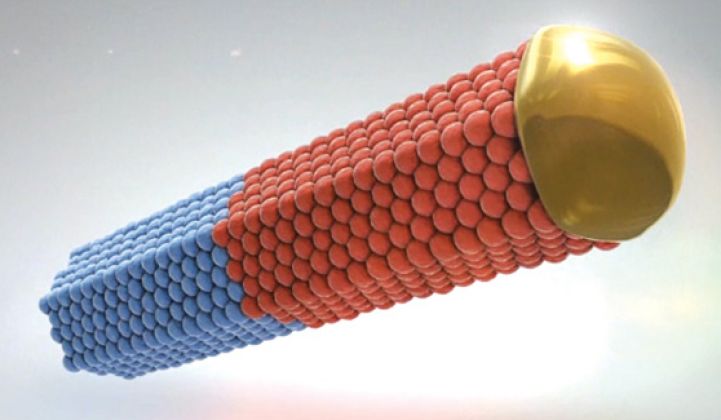
The researchers at NTNU have found a new way to make an ultrahigh power-per-weight ratio solar cell that is ten times more efficient than traditional solar cells by using GaAs in a nanowire structure.
GaAs solar cells are typically grown on a thick and expensive GaAs substrate, leaving little room for cost reduction.
“Our method uses a vertically standing semiconductor nanowire array structure on a cheap and industry-favorable Si platform to grow the nanowires,” says Helge Weman, a Department of Electronic Systems professor at NTNU.
“The most cost-effective and efficient solution is to grow a dual tandem cell, with a GaAs nanowire cell on the top grown on a bottom Si cell, which avoids the use of an expensive GaAs substrate. We have worked to minimize the cost of growing the top GaAs nanowire cell because it’s the GaAs fabrication cost that is one of the major issues that is currently holding back the technology,” Weman explains.
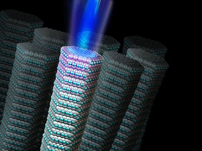
“The tiny footprint of the nanowire structure provides an additional benefit because it allows for high quality in crystals in the nanowire and the interface with the silicon. This helps improve the solar cell performance,” said Bjorn-Ove Fimland, a professor in the same department.
The development of this technology can be cost-effective with appropriate investments and industrial-scale R&D projects. Currently, the nanowires are grown using a technique known as MBE (molecular beam epitaxy), which is not a tool capable of mass production. However, using an industrial-scale tool like MOCVD, these nanowire-based solar cells can be mass-produced on a large scale (metal-organic vapor deposition).
When this product is combined with a Si cell, the efficiency of the solar cell can be increased by 40%, resulting in a doubling of efficiency compared to today’s commercial Si solar cells.
According to the researchers, their method could be reworked to grow nanowires on various substrates, potentially opening the door to a slew of new applications.
“We are exploring growing this type of light-weight nanowire structure on atomically thin two-dimensional substrates such as graphene. This could open up enormous opportunities to produce light-weight and flexible solar cells that can be used in self-powered drones, micro-satellites, and other space applications,” Mukherjee said.
The study was published in the American Chemical Society’s journal ACS Photonics.

 has developed a method for fabricating an ultrahigh material-efficient solar cell using semiconductor nanowires. If this is placed on top of a traditional silicon-based solar cell, it can double the efficiency of today’s Si solar cells while remaining inexpensive. “We have a new method of using gallium […]&media=https://wonderfulengineering.com/wp-content/uploads/2021/11/new-ultrahigh-material-efficient-low-cost-solar-cells-using-nanowires-l.jpg)