
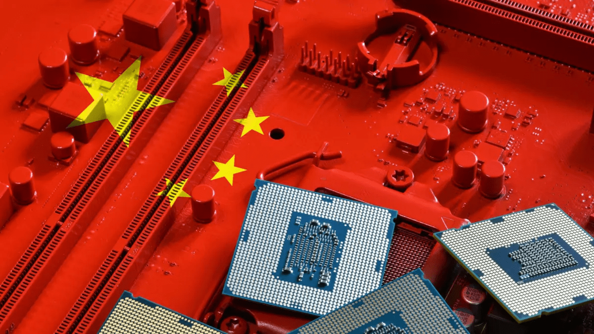
China has officially begun mass production of the world’s first non-binary chips, signaling a significant leap in computing technology. Developed by a team led by Professor Li Hongge at Beihang University in Beijing, this new generation of chips that are not only more energy-efficient and fault-tolerant but is also strategically designed to circumvent ongoing U.S. technology restrictions.
Modern chip design faces two formidable barriers: excessive power consumption and architectural limitations that make integrating new chips with older systems a challenge. Professor Li refers to these issues as the “power wall” and the “architecture wall.” Seeking a solution since 2022, his team introduced a novel system called Hybrid Stochastic Number (HSN) logic. This method blends traditional binary numbers with probability-based data representation to achieve higher efficiency without demanding more from the hardware.
Binary logic, the backbone of virtually all digital devices, performs computations using a strict system of 0s and 1s. While precise and reliable, large-scale binary operations require significant computational power and advanced hardware. On the other hand, probabilistic computing interprets high-voltage signal fluctuations over time to estimate values. Although less hardware-intensive and already applied in fields like image processing and neural networks, this method traditionally suffers from slower performance. The HSN approach was designed to bridge that gap, bringing the benefits of both without their drawbacks.
In 2023, Professor Li’s team rolled out a smart chip specifically for touch and display systems. Manufactured using Semiconductor Manufacturing International Corporation’s 110-nanometer technology, this chip marked the first real-world application of the hybrid computing model. Following this, a more advanced version aimed at machine learning was fabricated using a 28-nanometer CMOS process. These chips didn’t just rely on hybrid logic; they also employed in-memory computing to reduce the energy wasted in moving data between memory and processing units.
Additionally, their system-on-chip (SoC) design enabled them to perform multiple tasks simultaneously, an improvement over conventional single-task chips.
These new chips have already found practical uses. For instance, they are being integrated into smart touch systems where they can filter out background noise and detect subtle user inputs more accurately. Their ability to operate with minimal power makes them especially suitable for applications where efficiency and responsiveness are critical.
Professor Li stated that the chips currently achieve microsecond-level latency for on-chip computing, offering a solid balance between high-performance hardware and adaptable software programming. The research team is also developing specialized instruction sets and chip architectures tailored to hybrid probabilistic computing. These efforts are aimed at expanding the technology’s use into areas like speech and image recognition, artificial intelligence acceleration, and other complex computational tasks.
