
In a move that could reshape the landscape of computing, scientists at Peking University have unveiled a revolutionary transistor built entirely without silicon, a first-of-its-kind breakthrough that challenges the very foundation of modern electronics.
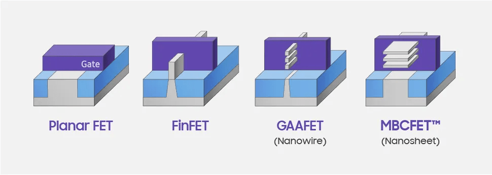
For decades, silicon has been the bedrock of digital computing, powering everything from smartphones to data centers. Its dominance, however, has been tied to a design paradigm reaching its physical and technological limits — the Fin Field-Effect Transistor (FinFET). These tiny vertical structures allowed engineers to keep shrinking chips while maintaining control over electrical current. But at sub-3 nanometer scales, even the finest silicon structures begin to struggle with power loss, overheating, and diminishing returns.
Recognizing this bottleneck, Professor Hailin Peng and his team at Peking University opted for a different approach rather than squeeze more out of silicon, they left it behind entirely.
“If chip innovations based on existing materials are considered a ‘short cut’, then our development of 2D material-based transistors is akin to ‘changing lanes’,” Peng told SCMP.

At the core of their breakthrough is a gate-all-around field-effect transistor (GAAFET), a design that wraps the gate around the channel on all four sides, offering even finer control of the electric flow compared to FinFETs. Though GAAFETs aren’t entirely new, what makes this one different is the material it uses: no silicon whatsoever.
The transistor incorporates a channel made from bismuth oxyselenide (Bi?O?Se) and a gate built from bismuth selenite oxide (Bi?SeO?), both of which belong to a new class of two-dimensional semiconductors — materials just a few atoms thick with outstanding electrical performance. Their unique properties enable electrons to move more rapidly through the structure, significantly boosting signal speed. At the same time, they reduce energy loss, leading to lower power consumption and less heat generation.
Additionally, the smoother interfaces between these materials result in fewer defects and more stable, reliable operation.
Peng likens the performance to “water moving through a smooth pipe,” as electrons flow with minimal resistance. The result? Their prototype transistor reportedly operates 40% faster than the latest 3-nanometer silicon chips while consuming 10% less energy.
This isn’t just about performance — it’s also about geopolitical independence. Amid U.S.-led export restrictions barring China from accessing cutting-edge chip fabrication tools, this breakthrough provides a way to leapfrog over current obstacles. Notably, the new transistor was made using existing fabrication platforms available in China, hinting at real-world scalability.
Yet challenges remain. Translating lab results into mass-market processors requires overcoming issues of durability, heat tolerance, and high-volume manufacturing. Building a transistor is one thing — integrating billions of them into functional chips is quite another.
Still, early signs are promising. Prototype logic units built using these transistors have demonstrated ultra-low voltage operation and strong voltage gain, both essential for real-world electronics. The team is now focused on scaling up production and refining their manufacturing techniques.
In their published study in Nature Materials, the researchers concluded: “This work demonstrates that 2D GAAFETs do exhibit comparable performance and energy efficiency to commercial silicon-based transistors, making them a promising candidate for the next technology node.”
