
Ali Javey and his team at the Department of Energy’s Lawrence Berkeley National Laboratory (Berkeley Lab) has created a transistor with a working 1-nanometer gate, which makes it the smallest transistor ever created, comparable with just one 50,000th the width of a strand of hair.
Javey, who is lead principal investigator of the Electronic Materials program in Berkeley Lab’s Materials Science said,
“The gate length is considered a defining dimension of the transistor. We demonstrated a 1-nanometer-gate transistor, showing that with the choice of proper materials, there is a lot more room to shrink our electronics.”
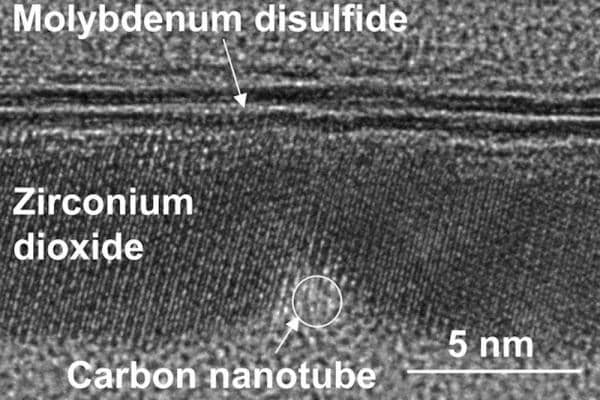
A lubricant, or molybdenum disulphide (MoS2), was combined with carbon nanotubes to create this transistor which measures to be just 1/20th the width of the top-end transistors available in the market.
The discovery is all the more impressive since theoretically it was believed that transistors couldn’t work below the width of 5-nanometers as it would induce quantum tunnelling.
What is Quantum Tunnelling?
As we all know, electrons usually travel as a “cloud of electrons” and the area of the cloud shows where the electron are most likely to be. However, transistors use the electron that jumps out of the cloud and is at a random location by tunnelling from one point to another. This electron is then amplified by an electrical signal which helps the outer electrons to into a higher orbit. This jump is conducted across to a collector, which creates the required electrical pulse, or a 1 in binary.
![How Transistors Work [Image Source: Explain That Stuff]](http://wonderfulengineering.com/wp-content/uploads/2016/10/how-transistor-works.png)
Challenges Making the Tiny Transistor
But the scientists countered this problem by using a different transition metal altogether. They used carbon, which until now was very hard to create with few enough imperfections to become a reliable transistor.
![World’s Smallest Transistor [Image Source: Berkeley Labs/Sujay Desai]](http://wonderfulengineering.com/wp-content/uploads/2016/10/transistor-610x343.jpg)
[Image Source: Berkeley Labs/Sujay Desai]
“The semiconductor industry has long assumed that any gate below 5 nanometers wouldn’t work, so anything below that was not even considered. This research shows that sub-5-nanometer gates should not be discounted. The Industry has been squeezing every last bit of capability out of silicon. By changing the material from silicon to MoS2, we can make a transistor with a gate that is just 1 nanometer in length, and operate it like a switch.”
Amazingly, the new transistor works seamlessly, providing an alternative to the traditional silicon transistors.
Javey, who is also a UC Berkeley professor of electrical engineering and computer sciences, commented,
“This work demonstrated the shortest transistor ever. However, it’s a proof of concept. We have not yet packed these transistors onto a chip, and we haven’t done this billions of times over. We also have not developed self-aligned fabrication schemes for reducing parasitic resistances in the device. But this work is important to show that we are no longer limited to a 5-nanometer gate for our transistors. Moore’s Law can continue a while longer by proper engineering of the semiconductor material and device architecture.”
The technology is not available for commercial use for now, but even the prospect of using such a small transistor heralds the dawn of even smaller and faster electronics in the future.

 has created a transistor with a working 1-nanometer gate, which makes it the smallest transistor ever created, comparable with just one 50,000th the width of a strand of hair. Javey, who is lead principal investigator of the Electronic Materials […]&media=https://wonderfulengineering.com/wp-content/uploads/2016/10/1nm_Carbon_Nanotube_transistor.jpg)